In recent years, with the rapid development of micro-nano science and technology, much progress has been made in the industrial area. However, to achieve batch manipulation of micro-nano structure with high density, large scale is one of the key challenging factors of realizing chip device. As everyone knows, the manipulation of single micro-nano structure could be well realized using the optical tweezers; however, manipulation on a large scale is time-consuming. Realization of high density, chip in one dimensional (1D) micro-nano array in a large scale with specific alignment orientation manufacturing is a crucial challenge of the integrated device. Zinc Oxide (ZnO), as an excellent member of the family of 1D micro-nano structures, is a direct wide band gap (3.3 eV) semiconductor with exciton binding energy of 60 meV. It can be applied to the laser emission units, field emitter transistors, photon detectors and generators. Zinc Oxide micro-nano structures can be utilized as highly efficient and stable exciton UV emission materials at room temperature. Until now, few studies have reported the preparation of horizontally aligned arrays of micro-nano structures via confined growth procedures. However, no study has been reported on the fabrication of large-scale horizontally aligned microstructure arrays with designed orientation and periodic distribution on p-type GaN to realize LED arrays.
Dr. Zhen Guo in SIBET presented a new method to obtain large-scale horizontally aligned ZnO microrod (the diameter of single ZnO microrod was 2 µm) arrays with periodic alignment on p-GaN layer via the combing technology. Horizontally aligned ZnO microrod arrays with uniform orientation and periodic distribution can be realized based on the conventional bottom-up method prepared vertically aligned ZnO microrod matrix via the combing method (Figure 1). When the combing parameters are changed, the orientation of horizontally aligned ZnO microrod arrays can be adjusted (θ= 90°or 45°) in a plane and a misalignment angle of the microrods (0.3° to 2.3°) with a low-growth density can be obtained. To couple the piezoelectric and wide-band gap semiconductor properties in ZnO, LEDs that are based on vertically and horizontally aligned ZnO microrods / p-GaN heterojunction were fabricated. Spot and line-shaped EL emission images demonstrated the different alignments of the ZnO microrods on p-GaN, as well as the different radiative recombination mechanisms of the emitted photons with different wavelengths at forward bias. Moreover, the emission color from UV-blue to yellow-green can be tuned by investigating the piezoelectric properties of the materials. In further, the proposed combing method can be applied to transform aligned distribution from vertical to horizonal horizontal orientation for micro- or nanostructures with any designed patterns and materials for building chips in devices. The related results have been published in the German Wiley International Journal Small, published online, DOI: 10.1002/smll.201402151, (SCI, IF= 7.514). (Website: http://dx.doi.org/10.1002/smll.201402151)
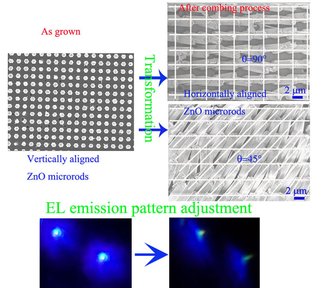
Figure 1. Transformation from vertically to horizontally aligned ZnO microrods is realized via combing technology. The orientation of the horizontally aligned ZnO microrods can be adjusted by changing combing parameters. Photoelectronic devices such as LEDs based on vertically and horizontally aligned ZnO microrods are fabricated, from which different emission patterns are captured.
